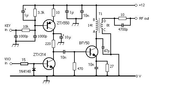
Keying and Driver Stages
The keying stage consists of a ZTX314 buffer with its collector supply switched by the ZTX550 keying transistor. The 15ohm resistor and clamp diode at the base of the buffer are to ensure the collector waveform is an approximate squarewave. The components in the base and collector of the ZTX550 are chosen to give a rise and fall time of the keyed rf of around 4ms and reduce keyclicks - on air use indicates these values are ideal.
The keying stage is fed to the BFY50 buffer which produces sufficient output for the pa transistor. A small TO5 heatsink is used on this transistor. The output power can be adjusted by changing the value of its 27ohm emitter resistor.
T1 is wound on a small ferrite core - a T50-2 is suitable.
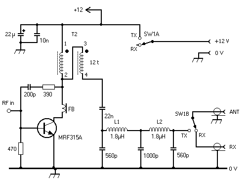
PA and Low Pass Filter
The PA uses a Motorola MRF315A 144MHz turnstile transistor - no particular reason for this choice, except that I had a few in the junk box. It is configured as a conventional class C stage. The output transformer T2 is bifilar wound and has an impedance ratio of 4:1, which is suitable for 5-10W when feeding a 50 ohm load. The same core type is used as for T1 in the driver stage, and a T50-2 should be suitable.
The low pass filter was modelled from the designs in the ARRL handbook and is designed for greater than 20dB attenuation of the second harmonic. The inductance values are fairly critical and should be checked with an inductance meter if possible. I used T200-2 cores, which are rather bigger than really required - again T50-2 should be OK.
A ferrite bead is required on the collector connection - a single wire through the bead. Without it the PA is unstable, as being a VHF transistor it has considerable power gain at these frequencies. Note also that the 22nF output coupling capacitor should be suitable to carry the rf current.
Construction
The transmitter is built in a suitable diecast box. A PL259 connector is used for the antenna, phone sockets for the keyer and receiver connections, and a double pole toggle switch for the receive/transmit switching. Current consumption is around one amp and any convenient 12V power supply can be used. Output power is around 6W.
The antenna is matched via my Yaesu FC901 ATU/Power meter which enables a good match to be obtained into the long wire antenna.